|
 |
|
| |
<%=FormatDateTime(Date(), vbLongDate)%>
|
|
News
August 2011
- Patent issued on new methods for fabrication of complex nanoscale devices
-
U.S. Patent 8,003,300, Methods for fabricating complex micro and nanoscale structures and electronic components and devices made by same, was awarded to K. Jain and U. Reddy on Aug. 23, 2011. The invention describes novel processing steps, methods and materials strategies for fabricating high-resolution structures for advanced electronic, optical and optoelectronic devices. The new methods are capable of making complex micro- and nano-scale structures, such as T-gates, gamma gates and shifted T-gates, having desired non-uniform cross-sectional geometries. The invention provides lithographic processing strategies for sub-pixel patterning in a single layer of photoresist and are useful for making and integrating device components comprising dielectric, conducting, metal or semiconductor structures having non-uniform cross-sectional geometries. The processing methods of this invention are complementary to conventional microfabrication and nanofabrication platforms, and can be effectively integrated into existing photolithographic, etching and thin-film deposition strategies, systems and infrastructure.
June 2011
- Lin completes Ph.D. degree
-
PMML graduate student Kevin Lin has successfully completed the requirements for the Doctor of Philosophy degree in Electrical & Computer Engineering. Lin's Ph.D. thesis, "Stretchable, Multimodal, Large-Area Sensor Arrays Fabricated Using Excimer Laser Photoablation Technologies" was accepted by the Graduate College on June 17, 2011.
Congratulations, Kevin! Well done!!
May 2011
- Patent issued on energy-efficient smart window technology
-
Professor Kanti Jain, graduate student Linus Jang and postdoctoral fellow Yoon Soo Han have been awarded U.S. Patent 7,940,457, Energy-efficient optoelectronic smart window, issued on May 10, 2011. The invention describes a new smart window technology that increases energy efficiency of building envelopes (windows, doors, skylights) by enabling programmable transmission control of the infrared and visible solar radiation into buildings, decreasing cooling costs during summer, heating costs during winter, and interior lighting costs all year. The technology is applicable to both commercial and residential buildings.
November 2010
- Jang completes Ph.D. degree
- PMML graduate student Linus Jang has successfully completed the requirements for the Doctor of Philosophy degree in Materials Science & Engineering. Jang's Ph.D. thesis, "Investigation of Physical and Electro-Optic Diffractive Structures for Energy-Efficient Smart Window Applications" was accepted by the Graduate College on Nov. 3, 2010. Congratulations, Linus! Well done!
July 2010
- Jain featured in 50 years of laser history milestones
- To highlight 50 years of innovations in lasers and laser applications, the website, LaserFest, presents a Timeline of Laser History Milestones (www.laserfest.org/lasers/history/timeline.cfm). Among the key milestones featured in this Timeline is the invention and demonstration of excimer laser lithography in 1982 by Professor Kanti Jain. >> Full article
April 2010
- Lin passes Ph.D. Preliminary Examination
- PMML graduate student Kevin Lin has successfully completed his Ph.D. Preliminary Examination. Congratulations, Kevin!
December 2009
- Jin completes M.S. degree
- PMML graduate student Hyunjong Jin has successfully completed the requirements for the Master of Science degree in Electrical and Computer Engineering. Jin's M.S. thesis, "Carbon Nanotube Strain Sensors with Wide Dynamic Range Fabricated on Flexible Substrates by Novel Processing Techniques" was accepted by the Graduate College on November 20, 2009.
Congratulations, Hyunjong! Well done!!
April 2009
- Patent application filed on new spatial light modulator technology for lithography and displays
- K. Jain, J. Chae, K. Lin and H. Jin, Patterning Mirror Arrays for Maskless Photolithography and Image Display, U.S. Pat. pending.
March 2009
- PMML graduate student Kevin Lin has been awarded the 2009-2010 Ernest A. Reid Fellowship Award in Electrical Engineering. This award is given to a student or students with exceptional promise for an academic career, particularly demonstrating interest in and capability for the instructional program. The objective of the award is to encourage students to consider an academic career. This Fellowship provides a cash award of $5,000.
February 2009
- Jain elected to The National Academy of Engineering
- Professor Kanti Jain has been elected to The National Academy of Engineering (NAE), "For contributions to the development of high-resolution, deep-ultraviolet excimer lithography for microelectronic fabrication." NAE was established in 1964 under a charter from the National Academy of Sciences as a parallel organization of outstanding engineers. Election to the NAE is among the highest professional distinctions in engineering.
"Professor Kanti Jain's contributions are fundamental to how semiconductor devices and chips are manufactured today," explained Ilesanmi Adesida, dean of the College of Engineering. "His work has broad impact on computers, cell phones, and many modern day tools and conveniences. It is fitting that he is being elected into the Academy for his achievements."
"This prestigious honor is an indication of Professor Jain's pioneering contributions to the field of optical engineering," said Richard Herman, the chancellor of the Urbana-Champaign campus. "We are extremely proud of his accomplishments, which are emblematic of the continuing legacy of excellence of our university."
(See also: http://engineering.illinois.edu/news/?xId=0637078407140686
and http://www.ece.illinois.edu/news/headlines/hl-jain-nae.html)
December 2008
- Patent application filed on new patterning methods for fabrication of stretchable structures
- K. Lin and K. Jain, Patterning Methods for Stretchable Structures, U.S. Pat. pending.
December 2008
- Jin passes Ph.D. Qualifying Examination
- PMML graduate student Hyunjong Jin has successfully completed his Ph.D. Qualifying Examination. Congratulations, Hyunjong!
December 2008
- Jang passes Ph.D. Preliminary Examination
- PMML graduate student Linus Jang has successfully completed his Ph.D. Preliminary Examination. Congratulations, Linus!
November 2008
- PMML Initiative on Energy-Efficient Smart Window Technology Funded under Grainger Program in Emerging Technologies
- Professor Kanti Jains proposal on a novel Energy-Efficient Optoelectronic Smart Window Technology has been selected by the College of Engineering for funding under the Grainger Program in Emerging Technologies. The program was created by the Grainger Foundation to promote the transition of new academic developments in engineering into commercially viable products and services.
Current worldwide energy resources are becoming scarcer and more expensive every year while barriers (technological, financial, and political) to developing new energy sources remain significant. According to the Department of Energy, the cost of energy used for heating, cooling, and lighting in commercial and residential buildings in 2005 was a staggering $416 billion, a figure that is certainly much higher now. It has been further estimated that annual energy costs due to inefficient windows exceed $50 billion, and those for interior lighting, $70 billion. We are developing a novel smart window technology that will reduce losses, increase efficiency, and enable recycling of valuable energy resources. Our technology overcomes limitations of previous approaches, leading to dynamically programmable, energy-efficient window systems. This novel technology is an optoelectronic window system based on polymer blazed diffraction gratings constructed by microelectronic fabrication processes. The gratings are designed to enable dynamic control of the transmission of the visible and near-infrared solar radiation through the smart window. Since the benefits of the new technology include lower cooling costs during summer, lower heating costs during winter, and lower interior lighting costs all year, it will be applicable globally, without geographic or seasonal limitations.
August 2008
- Patent application filed on new technology for energy-effcient smart windows for buildings
- K. Jain, L. Jang and Y. Han, Energy-Efficient Optoelectronic Smart Window, U.S. Patent pending.
April 2008
- Lin passes Ph.D. Qualifying Examination
- PMML graduate student Kevin L. Lin has successfully completed his Ph.D. Qualifying Examination. Congratulations, Kevin!
April 2008
- Lin completes M.S. degree
- PMML graduate student Kevin L. Lin has successfully completed the requirements for the Master of Science degree in Electrical and Computer Engineering. Lin's M.S. thesis, "Large-Area, Stretchable, Multimodal Sensor Skins Fabrictaed by Novel Process Technologies and Heterogeneous Integration," was accepted by the Graduate College on April 15, 2008.
Congratulations, Kevin! Well done!!
March 2008
- Jain awarded David Richardson Medal of Optical Society of America
- Professor Kanti Jain has been awarded the David Richardson Medal by the Board of Directors of the Optical Society of America for achievements in the field of optical engineering. Each year OSA presents the award to one individual chosen for his "dedication, ingenuity, and perseverance in attaining the highest level of scientific achievement in their chosen fields." The award recognizes those who have had significant influence primarily in the commercial and industrial sector of optical engineering. Dr. Jain is specifically honored for his "pioneering contributions to the development of high-resolution optical microlithography technologies, particularly for the invention and development of excimer laser lithography technologies and systems for production of microelectronic devices," according to the OSA citation. Excimer laser lithography systems are now used worldwide for semiconductor integrated circuit manufacturing. In addition, in the 1990s, Dr. Jain developed the technologies for large-area lithography that are widely used today in the production of flat-panel displays and televisions.
(See also: www.ece.uiuc.edu/news/headlines/hl-jain-medal.html)
February 2008
- Research on new ITO patterning method featured in SPIE Newsroom
- The successful research effort in the PMML group on development of a new patterning method for thin films of ITO by excimer laser photoablation processing has been featured in SPIE Newsroom. The new method is attractive in the fabrication of flat-panel displays and other microelectronic devices.
"Low cost patterning process for flat panel displays," SPIE Newsroom, 8 February, 2008
(See also: http://spie.org/x19491.xml?highlight=x2408)
December 2007
- Research on new display fabrication patterning technique featured in ECE Headline News
- The successful research effort in the PMML group on development of a new patterning technique for thin films of ITO and other materials by excimer laser photoablation processing has been featured as a Headline News story on the Department of Electrical & Computer Engineering website. The new method, developed by Professor Kanti Jain and postdoctoral researcher Junghun Chae, is potentially attractive in lowering production costs in the fabrication of flat-panel displays and other microelectronic devices. The inventors have applied for a patent for the technology and are pursuing commercialization efforts.
"New technique simplifies flat-panel display fabrication," ECE headline News, December 7, 2007.
(See: www.ece.uiuc.edu/news/headlines/hl-jain-display.html)
September 2007
- Reddy completes M.S. degree
- PMML graduate student Uttam Reddy has successfully completed the requirements for the Master of Science degree in Electrical and Computer Engineering. Reddys M.S. thesis, "Subpixel Resolution Nanolithography and Applications in Advanced Semiconductor Devices," was accepted on September 17, 2007, making him the first graduate of the PMML group.
Congratulations, Uttam!!!
September 2007
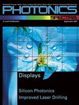
- Research on new ITO patterning method featured in Photonics Spectra
|
|
The successful research effort in the PMML group on development of a new patterning method for thin films of ITO by excimer laser photoablation processing has been featured in Photonics Spectra. The new method is attractive in the fabrication of flat-panel displays and other microelectronic devices.
"Patterning Films with Fewer Steps," Photonics Spectra, Vol. 41, No. 9, p. 112, September 2007. (See also: www.photonics.com/content/spectra/2007/September/LED/88889.aspx)
|
July 2007
- Patent application filed on new technology for fabrication of nanoscale dual damascene structures
-
K. Jain and U. Reddy, Methods for Making Nanoscale Dual Damascene Profiles and Devices Made by Same, U.S. Pat. pending.
June 2007
- Paper on new ITO patterning method for flat-panel display fabrication published in Applied Physics Letters
- J. Chae, S. Appasamy and K. Jain, Patterning of indium tin oxide by projection photoablation and lift-off process for fabrication of flat-panel displays, Appl. Phys. Lett., Vol. 90, p. 261102 (2007).
April 2007
- Reddy passes Ph.D. Qualifying Examination
- PMML graduate student Uttam Reddy has successfully completed his Ph.D. Qualifying Examination.
April 2007
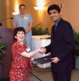
- Reddy wins Perry Fellowship
-
|
|
PMML graduate student Uttam Reddy has been awarded the Harriett and Robert Perry Fellowship. The Perry Fellowship was created in 1996 by a gift from Robert Perry, an alumnus of the Department of Electrical and Computer Engineering. Mr. Perry and his late wife wished to establish a fund that would help to ease the financial burden for meritorious students in the ECE department seeking an advanced degree. This Fellowship provides a cash award of $5,000.
|
March 2007
- Jain group and collaborators win $6.3 million DARPA award for proposal on disruptive manufacturing technology
-


|
|
A team comprising University of Michigan at Ann Arbor (Professors Suman Das and John Halloran), University of Illinois at Urbana-Champaign (Professor Jain), Anvik Corporation, and Honeywell Aerospace has received a $6.3M, four-year award from DARPA for their proposal "Direct Digital Manufacturing (DDM) of Airfoils" in response to DARPA’s solicitation on "Disruptive Manufacturing Technologies." DDM of airfoils will be achieved by the processing of photocurable ceramic resins through a new direct digital manufacturing technology known as Large Area Maskless Photopolymerization (LAMP) being developed by the team. LAMP combines layered manufacturing of complex three-dimensional objects by solid freeform fabrication (SFF) with the fine-feature resolution and high throughput of massively parallel scanning maskless lithography to achieve a disruptive breakthrough in part build speed and feature definition. LAMP promises an unprecedented ability to rapidly manufacture parts that have macroscale exterior dimensions and microscale interior features. (See also: www.ece.uiuc.edu/news/headlines/hl-jain-grant.html) |
January 2007
- Patent application filed on cost-effective fabrication methods for flat-panel displays
- K. Jain, J. Chae and S. Appasamy, High-Throughput, Low-Cost, Dual-Mode Patterning Methods for Large-Area Substrates, U.S. Pat. pending.
April 2006
- PMML graduate student Uttam Reddy has received the Olesen Award of the Department of Electrical and Computer Engineering, given to a graduate student for excellence in undergraduate teaching. The award is made each semester to one or more graduate students teaching in the ECE department to recognize an outstanding effort in undergraduate teaching. The award was set up as part of the Harold L. Olesen Fund for Undergraduate Instruction Improvement.
February 2006
- Jain elected Fellow of IEEE
- Professor Kanti Jain has been conferred the title of IEEE Fellow by the Board of Directors of the Institute of Electrical and Electronics Engineers for his work on high-resolution excimer laser lithography. As presented in an IEEE press release: "An important part of the IEEE’s mission is to recognize the professional achievements of its members. The Institute’s highest honor is the rank of IEEE Fellow, bestowed on members who have contributed ‘to the advancement or application of engineering science and technology ’." The technology of excimer laser lithography was invented and developed by Jain at IBM in the 1980’s and is now used worldwide in semiconductor chip production.
|
|
|
|